PCB assembly and testing

Tony
Site Admin
Posts: 949
Joined: Tue Jul 24, 2012 8:05 pm

Re: PCB assembly and testing

Post by Tony »

Assembling the nixie tube sockets:

Image

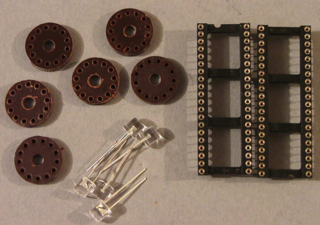
Using wirecutters or pliers carefully break the turned pin sockets out of the plastc housing:

Image

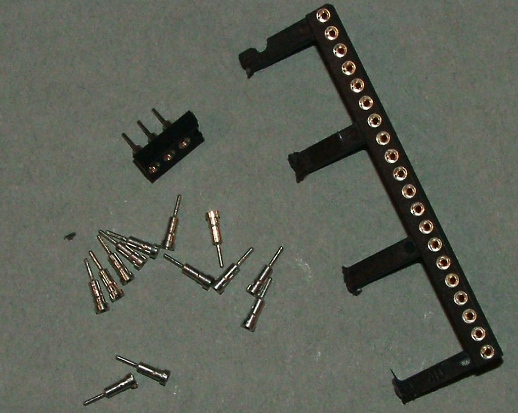
Push the pins into the holder:

Image

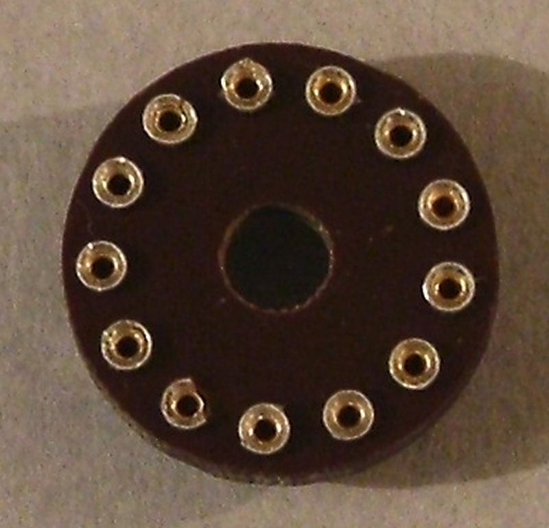
Once made, drop them into the V1-5 positions on the PCB and solder them in place.

Now fit the LEDs through the centre hole so they sit on top of the socket. NOTE that these are polarised and must be fitted the right way round. The SHORT PIN faces to the LEFT of the PCB when viewed from the front.

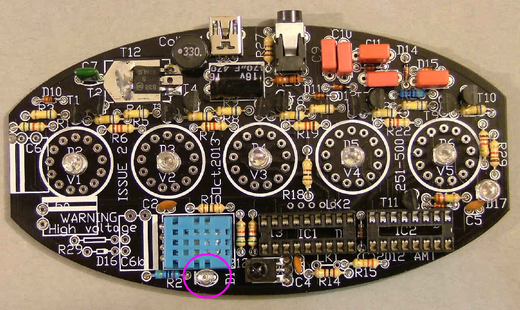
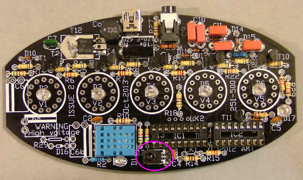
D17 is no longer used.
Tony
Site Admin
Posts: 949
Joined: Tue Jul 24, 2012 8:05 pm

Re: PCB assembly and testing

Post by Tony »

Fit the black plastic transistors marked 'MPSA92' in locations marked for T1,3,5,7 and 9 as shown: NOTE these are polarised and must be fitted the right way round. There is a flat mark on one side of the body, this flat side faces to the LEFT of the PCB when viewed as shown in the photograph.

The may also be marked 'KSP92' or just 'A92'


Image
Tony
Site Admin
Posts: 949
Joined: Tue Jul 24, 2012 8:05 pm

Re: PCB assembly and testing

Post by Tony »

Fit the black plastic transistors marked 'MPSA42' in locations marked for T2,4,6,8,10 and 11 as shown: NOTE these are polarised and must be fitted the right way round. There is a flat mark on one side of the body, this flat side faces to the RIGHT of the PCB when viewed as shown in the photograph.

They may also be marked 'KSP42' or just 'A42'.


Image
Tony
Site Admin
Posts: 949
Joined: Tue Jul 24, 2012 8:05 pm

Re: PCB assembly and testing

Post by Tony »

Fit the green resin 4n7 capacitor in the location marked for C7 as shown:

Image
Tony
Site Admin
Posts: 949
Joined: Tue Jul 24, 2012 8:05 pm

Re: PCB assembly and testing

Post by Tony »

Fit the blue, green or black aluminium can 470u or 330u 10V capacitor in the location marked for C8 as shown: NOTE this is polarised, the negative terminal is marked with a white band. This faces towards the BACK of the PCB when viewed as shown.


Image
Tony
Site Admin
Posts: 949
Joined: Tue Jul 24, 2012 8:05 pm

Re: PCB assembly and testing

Post by Tony »

Carefully fit the USB socket, it may be a little tight but don't push too much or you may damage the pins.


Image
Tony
Site Admin
Posts: 949
Joined: Tue Jul 24, 2012 8:05 pm

Re: PCB assembly and testing

Post by Tony »

Fit the 3.5mm jack socket marked SK2:


Image
Tony
Site Admin
Posts: 949
Joined: Tue Jul 24, 2012 8:05 pm

Re: PCB assembly and testing

Post by Tony »

Fit the 3mm IR LED in the space marked D1 as shown, leaving enough lead length for it to sit over the square marked 'IC4', pointing slightly to the right. NOTE this is polarised and must be fitted the right way round. There is a flat mark on the side of the LED body, this flat side faces to the TOP of the PCB when viewed as shown in the photograph, with the short lead going to the pad under R2.

Lleave about 3mm of lead under the LED to allow the angle to be adjusted:

Cut a short piece of heatshrink sleeving (about 12mm) to cover the LED and prevent light from the sides of it being picked up by the sensor.

Image
Tony
Site Admin
Posts: 949
Joined: Tue Jul 24, 2012 8:05 pm

Re: PCB assembly and testing

Post by Tony »

Fit the IC sockets SK3 and 4 as shown, making sure the notches face D8 as marked on the PCB:

Image
Tony
Site Admin
Posts: 949
Joined: Tue Jul 24, 2012 8:05 pm

Re: PCB assembly and testing

Post by Tony »

Fit IC3 as shown (the domed black plastic or silver metal 3 legged block), bending it to face slightly to the left of horizontal. The exact angle may need to be adjusted later for best sensor response.


Image
Post Reply